
12/03 Day 3 🎄
Never too many acronyms :P


Welcome back to Unwrapping TPUs ✨!
Yesterday, we established that the TPU v1 has a powerful systolic array allowing for efficient matrix multiplications in regards to data flow, as well as data buffering techniques which allow for faster data reads. The efficiency of the TPU arises not only from the architecture behind it, but also the minimalist, yet robust, instruction set and pipelining associated with it. Today, we aim to outline the TPU’s instruction set and pipelining, and how that allows for massive parallelism.
Systolic Array Recap:
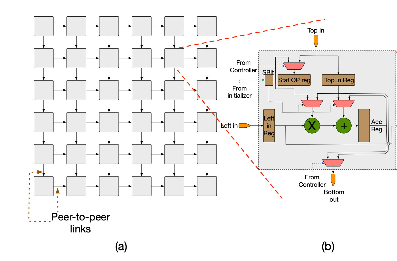
(Samajdar, Pellauer, and Krishna)
The TPU’s central purpose is to feed dense MatMuls into a 256 x 256 dimension systolic array located in the Matrix Multiply Unit (MMU). Activation data is streamed in from the left and weight tiles are streamed in from the top in waves at every clock cycle (like a heartbeat). To be clear, this allows for a remarkable 65,536 MACs for 8-bit integers every cycle, but this MMU systolic array is not well suited for general-purpose computations. Additionally, note that the v1 architecture is great for densely packed MatMuls,
This leads us to our first point regarding the TPU Instruction Set Architecture or ISA for short. Let’s start with understanding the CPU.
CPU Fundamentals: ISA and Pipelining
The classical CPU’s ISA is nothing more than a definition of instructions that the CPU executes. The ISA defines the contract between the hardware and the software, specifying registers, memory access, and data types (Whalley, 1999).
The whole process that the ISA relies on can be broken down into three fundamental steps: fetch, decode, and execute.
Fetch: The Program Counter (PC) holds the memory address of the next instruction to be read from memory. The CPU uses this address to fetch the instruction word. After the instruction is retrieved, the PC is typically incremented to point to the subsequent instruction in the program sequence.
Decode: The fetched instruction is loaded into the Instruction Register (IR). The control unit then reads a section of this instruction, called the opcode (operation code), which defines the necessary instruction the CPU should execute (e.g., ADD, AND, JUMP). The decoding stage translates the opcode into a sequence of control signals for the execution units.
Execute: The control signals initiate the required action—an arithmetic operation, a logical test, or a memory transfer.
Thus, the ISA instruction is just an n-bit number (usually n is 16, 32, or 64, depending on the underlying CPU architecture) that specifies an instruction the CPU should execute at a given time. Naively, this all happens sequentially, where the CPU completes all three steps for instruction N before starting instruction N +1, however modern CPUs use a trick called pipelining to increase efficiency.
Intuitively, the idea of only sequentially executing instructions makes good sense because we are just loading in relevant instructions, but let’s give an analogy to break it down. Consider you are a cook making 3 different meals for a restaurant. For each dish we have to: prep, cook, and clean. Sequential execution would have us prep, cook, and clean for the first dish, and then we would have to repeat these steps all over again for the second and third dishes. Pipelining is essentially having us begin prep for dish 2 as soon as dish 1 is ready to cook. Then, when dish 1 is finished cooking and moves onto the cleaning phase, we can begin cooking dish 2. This technique allows us to increase the dishes completed per unit time.
Back to the hardware, pipelining a CPU allows us to increase throughput through use of instruction-level parallelism or ILP. By considering this overlap of instructions, we arrive at the formula:
GPU vs TPU:
So how does this connect to the TPU? Now that we’ve covered the CPU and it’s efficiency in pipelined sequential settings, we naturally look towards more parallel implementations. Multi-core CPUs spearheaded the idea of superscalar processing, but the rise of GPUs brought on a whole new dimension of efficiency in parallel computing possibility.
Extremely briefly, GPUs are considered more general purpose parallel computing machines that specialize also in MatMuls. We encourage you to look through this glorious guide to GPUs written by Modal for more exploration: https://modal.com/gpu-glossary. A GPU contains many smaller cores or streaming multiprocessors (SMs). Each SM contains a tensor core (much smaller than the TPU MMU) of it’s own and a set of warps (32 thread bundles). In turn, every SM is much more flexible and totally independent to act on hundreds of thousands of separate tasks at once.
Thus, a GPU emphasizes parallelism in the sense that we have many many workers doing independent tasks at once (Single Instruction Multiple Thread (SIMT) parallelism) among many other efficiencies that we won’t get too deep into (especially with Blackwell, Rubin, and beyond). Since the Tesla generation, GPUs have become turbo-super-ultracharged and the internal workings are somewhat of a mystery. We don’t even get to see the bottom assembly level as these details are abstracted away in the CUDA development environment.
A TPU in comparison is one giant machine where it has many many cogs turning at the same time. The TPU’s power comes from fixed-function spatial and dataflow parallelism as well as massive spatial reuse of activations and weights.
Recently, we had a question brought up on Twitter, which astutely asked about the potential for a RISC-V TPU architecture TPU. Let’s break that down.
In the TPU v1 floorplan, we see that deliberate sacrifices are made in both layout area and networking to optimize around the MMU’s systolic array for the sole purpose of dense MatMuls. The philosophy of the TPU microarchitecture is to keep the matrix unit busy.
The end of Dennard Scaling and Moore’s Law meant we need to lower the energy per instruction to match the performance per watt (PPW) densities in prior decades. Especially as AI workloads scale and models grow in size, this means that to create order-of-magnitude performance improvements, we sacrifice generality in instruction set and must increase the number of arithmetic operations per instruction.
Unlike a GPU, which is far more flexible in general purpose parallel computing applications, a TPU is rigid in operational condition and type (in true ASIC fashion) to achieve massive parallelism on the problem of large and dense MatMuls.
TPU ISA:
Accelerators, like the TPU v1, therefore, follow a Complex Instruction Set Computer (CISC) architecture that focus on only managing the massive parallelism needed to feed the MMU. If the TPU was designed with RISC in mind, we would be trading off this bespokeness and performance due to the need to decompose every high-level matrix operation into thousands of smaller scalar instructions: the volume of these instructions would overwhelm the instruction stream and eliminate the throughput advantage.
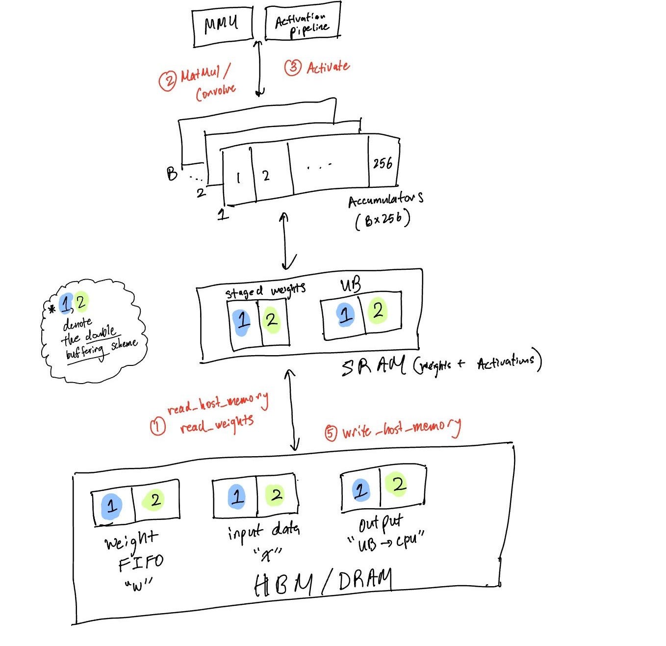
The TPU’s CISC instruction set focuses on high-level operations directly related to the MMU via important hardware blocks such as the Unified Buffer (UB), Weight FIFO, and Vector Processing Unit (VPU). The VPU, to clarify, is where all per-element activation work (non-linear functions) sit to apply to accumulator outputs. The following are the key shortlist of operations being done, we break them down in operational four-stage pipelined order (there are around 20 CISC operations total):
We first setup with the following:
(1) Read Host Memory: (Read from host CPU memory to UB for initial data input into MMU)
Read Weights: (Read from Weight Memory to Weight FIFO)
Note that since the data being read is from DRAM off-chip (HBM in modern TPUs) to the on-chip UB’s SRAM and Weight FIFO, this takes quite a bit of time. Thus, the double buffering scheme for this phase is pipelined the next step’s math.
Extra: In the case that read times are super long, we run into a bandwidth bound scheme! Extra Extra: bandwidth bound refers to the memory bandwidth being exhausted i.e. we can’t fetch enough data fast enough (not necessarily a bad thing).
Once loaded (and receiving the next batch of data), we then continuously feed the from the Weight FIFO and UB into the top and left of the MMU to do our large dense MatMuls:
(2) MatMul / Convolve: (MAC operations inside of the MMU, fed into the Accumulator for updating)
For every cycle of Accumulator update, we feed into the VPU and then pass it’s results to the UB:
(3) Activate: (Non-linear functions applied to Accumulator results in VPU)
Finally, once complete, we then:
(4) Write Host Memory: (Write back to host CPU memory from UB)
Note here that since SRAM in the UB is much smaller than the off-chip DRAM being accessed, we require much lower Arithmetic Intensity (operations / byte) to achieve peak utilization. Efficiently utilizing SRAM becomes the name of the game!
Since these are CISC instructions, say a single MatMul or Convolve instruction may take hundreds or thousands of cycles to execute. This is the secret sauce, however, as the TPU’s CISC architecture allows the host CPU to be freed from issuing millions of low-level instructions (Deterministic Execution). In turn, the TPU is able to meet low-latency 99th percentile response-time requirements for Google’s data center applications.
Referencing the TPU v2+ ISA architecture, a way to visualize the TPU v1 4-stage pipeline in action across memory levels is as follows (if you want to see v2+ in a nifty GIF written up by the DeepMind team here):
(Austin, J., Douglas, S., Frostig, R., Levskaya, A., Chen, C., Vikram, S., Lebron, F., Choy, P., Ramasesh, V., Webson, A., & Pope, R.)
Do note that in the DeepMind JAX / Pallas documentation the right half of the diagram references scalar units like SREG / SMEM which were added in subsequent generations of the TPU for complex control flow. Note of a note here, in the case that the JAX / Pallas / TPU team who made the blog is reading it, hope we got the main gist down (big fans of your work)!
Additional operations in the CISC ISA of the TPU include:
Read Host Memory: host CPU DRAM to UB transfer
Write Host Memory: UB to host CPU DRAM transfer
Synchronize (local TPU) Host Memory: Wait for TPU operation completion
Synchronize (host CPU): Coordinate memory transfers
2x Interrupt Host: Signal to host CPU the TPU is done
Nop: No-operation a.k.a do nothing
Halt: Graceful TPU shutdown
Synchronize: Keep track of instruction place before interrupting in memory synchronization
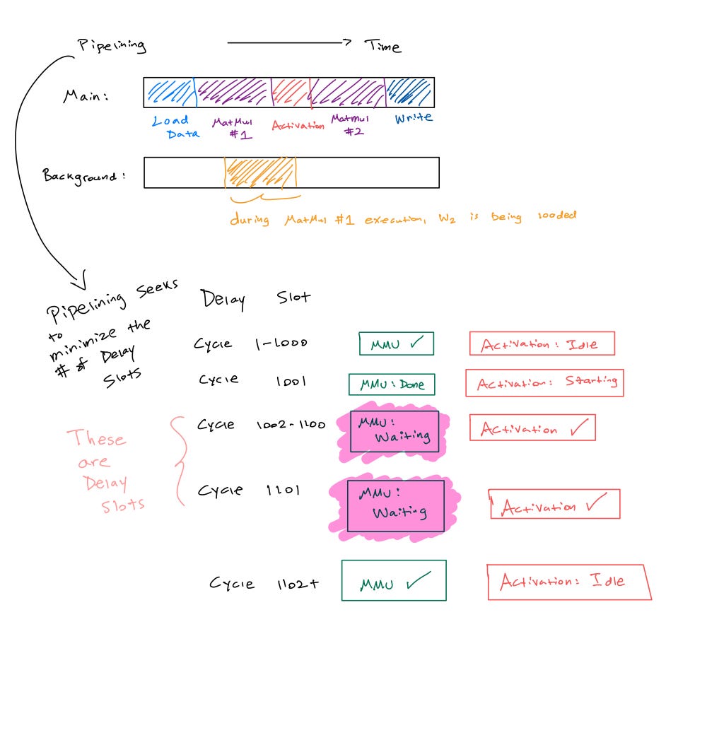
Of course, this deep pipelining isn’t without challenges. The MMU will stall if the input activation or weight data is not ready. The most interesting cases occur when activations from one network layer must complete before the next layer’s matrix multiplications can begin. We see a “delay slot” which essentially means the matrix unit waits for explicit synchronization before safely reading from the Unified Buffer (Jouppi et al., 2017). A sneak peak for the future: the TPU compiler is in charge of managing these synchronization points!
In brief, the beauty of combining systolic arrays with this pipelining approach is that once data enters the systolic array, additional control logic on how data should be processed is not required, and when given a large enough systolic array, there’s no memory read/writes other than the input and output (Ko, 2025).
FFN Forward Pass Walkthrough
Now that we understand the TPU’s pipelining and instruction set, let’s walk through an example FFN (Feed Forward Network) Forward Pass. This will illustrate how the TPU’s architecture, pipelining, and CISC instructions work together in practice!
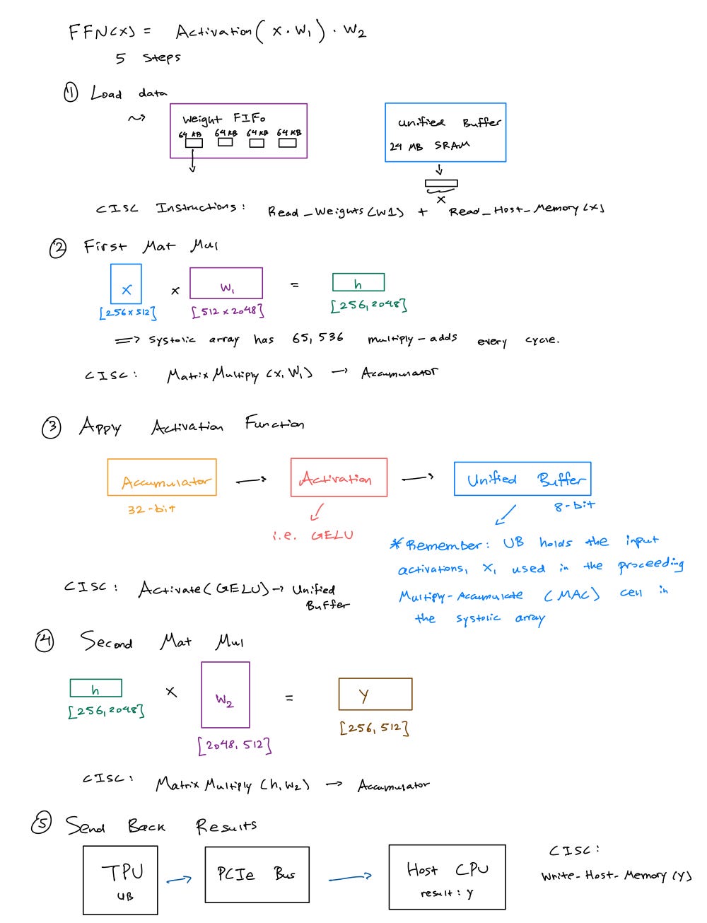
A typical FFN layer in a transformer consists of two matrix multiplications with an activation function in between them. the input has shape [batch_size, dim_model], matrix 1 has shape [dim_model, d_ff] (usually dim_ff = 4 × dim_model) and matrix 2 has shape [dim_ff, dim_model].
Let’s say we’re processing a batch of 256 sequences with d_model = 512 and d_ff = 2048.
The Instruction Trace: the entire FFN layer compiled down to roughly 20 CISC instructions look something like this:
Setup:
Read_Weights(W_1), Read_Host_Memory(x)
First matmul: MatrixMultiply(x, W_1) → Accumulator
Activation: Activate(GELU) → Unified Buffer
Second matmul: MatrixMultiply(h, W_2) → Accumulator
Writeback: Write_Host_Memory(y)
Comparing this to RISC, we’d need millions of scalar instructions for the same work. CISC keeps the instruction stream simple while the 256×256 systolic array handles the parallelism underneath.
Pipelining Overlap: these instructions don’t run sequentially. While MatMul #1 executes, W_2 weights are already loading (double buffering). While the activation is applied, the next weights stream into the Weight FIFO. While writing results to host, the next layer’s setup can begin. This overlap is why the TPU achieves high utilization. Without it, we’d wait for each weight load. With pipelining, memory transfers hide behind compute and allow the systolic array to reach its potential.
The Delay Slot: one place we can’t overlap: layer boundaries. Layer N’s output must pass through the activations and write to the Unified Buffer before Layer N+1 can read it. The MMU stalls during this window ~ this is exactly the delay slot! The compiler inserts synchronization instructions to enforce these dependencies.
The overarching philosophy holds: keep the matrix unit busy, and everything else follows.
Works Referenced
Samajdar, Pellauer, & Krishna, Self-Adaptive Reconfigurable Arrays (SARA): Using ML to Assist Scaling GEMM Acceleration
Jouppi, N. P., Young, C., Patil, N., Patterson, D., et al. (2017). In-Datacenter Performance Analysis of a Tensor Processing Unit. In Proceedings of the 44th International Symposium on Computer Architecture (ISCA).
Kate, S. (2021). A Tensor Processing Unit Design for FPGA Benchmarking [Master’s thesis, University of Texas at Austin].
*Ko, H. (2025). TPU Deep Dive. https://henryhmko.github.io/posts/tpu/tpu.html*
*Austin, J., Douglas, S., Frostig, R., Levskaya, A., Chen, C., Vikram, S., Lebron, F., Choy, P., Ramasesh, V., Webson, A., & Pope, R. (2025). How to Scale Your Model. Google DeepMind. https://jax-ml.github.io/scaling-book/tpus*