
12/16: Day 16 🎄
ISA ISA Play!


Welcome back to Unwrapping TPUs ✨
We’ve spent a lot of time wondering about the exact details of each of our logical blocks, from the Weight FIFO to the Accumulator. Along the way, our Verilog has strung along quite a few control signals and enables. Today, we begin the work of cleaning up the control signals and develop the ISA serving the basis for our tiny^2 TPU.
What is an ISA?
An ISA or instruction set architecture is what binds the compiler for your higher-level code and the underlying hardware’s microarchitecture. Architecture refers to the hardware guarantee and microarchitecture is a subset of the architectural choices made for a specific hardware function.
Given a source program that you as a software developer write, an ISA usually binds to an intermediate representation (IR) of fewer constructs and longer instruction code sequence, before converting that IR to machine level instructions.
In the case of our TPU design, there is especially no such thing as a general purpose ISA. Given it’s extremely focused utility as a MatMul machine, our ISA follows a CISC setup of highly powerful but specific instructions. Our priority is to satiate the MMU as quickly and efficiently as possible for optimized inference.
Current Control Signal Inventory
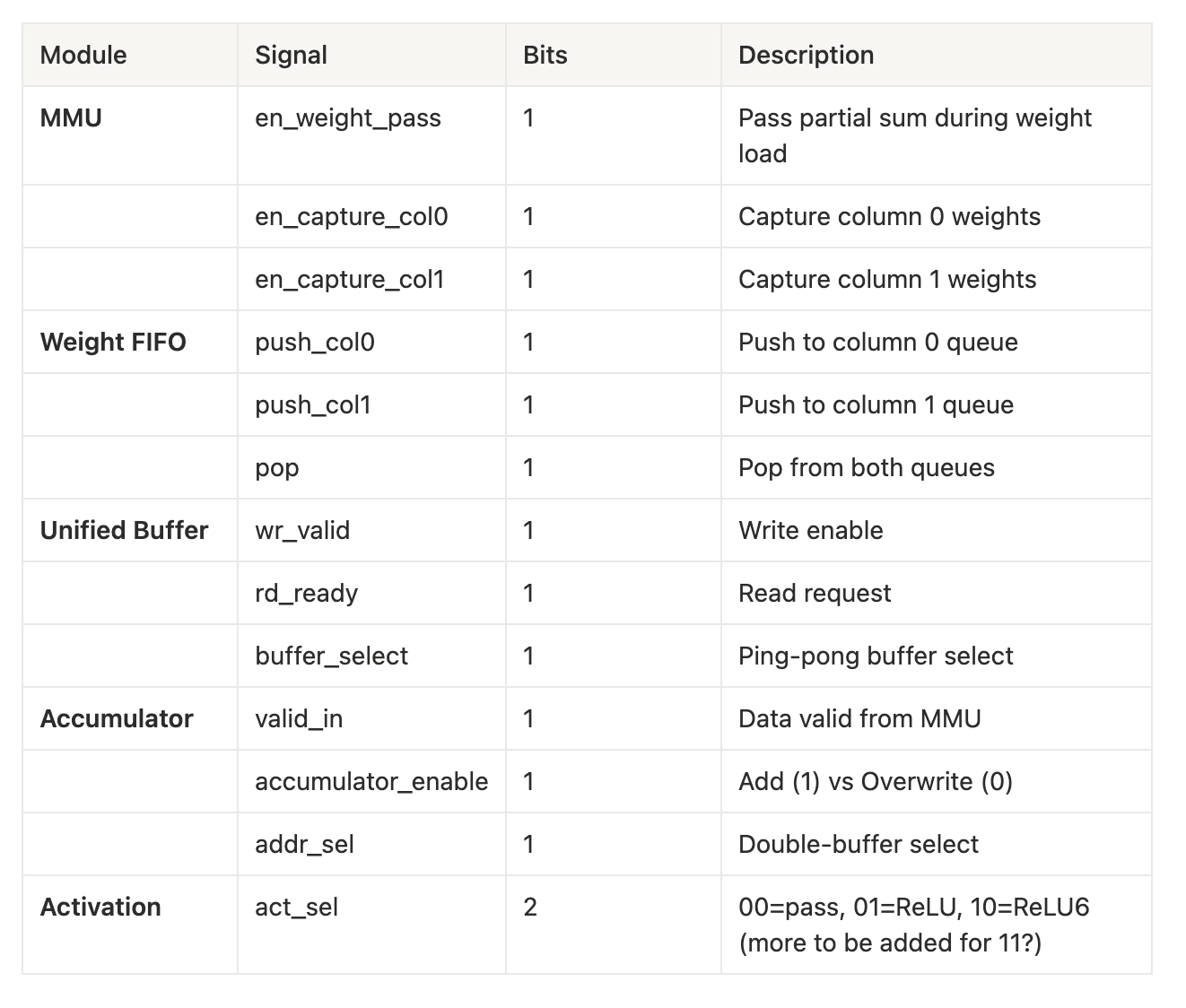
Thus, in total we have 14 independent control bits, while excluding data buses and config registers. As we expand the systolic array beyond it’s current 2 x 2 setup, using fixed microcode ROM instructions would not work as the ROM size would expand quadratically with the array dimension. Additionally, any change to the array size would require a unique microcode table to map instructions.
In our design for this tiny^2 TPU, we therefore look towards a system of parametrized operations split between user-facing instructions and the lower-level control signals, flexible to hardware dimension.
Parametrized ISA Operations
Ideally, every operation in our tiny^2 TPU follows scales linearly according the array dimension of 2 (as per our mini 2 x 2 implementation specs). Weight loading takes 3 (3 = 2+1) cycles since each column is staggered and receives its weight in the MMU as a diagonal wavefront. The compute phase similarly takes 3 cycles, with 2 cycles to fill in completely (weights and activations simultaneously) and 1 cycle to drain results when passed to the Accumulator. Subsequent steps to traverse through the activation pipeline add additional cycles.
Today, we break down a sketch of the very first level of user-facing instructions.
User-facing Instruction Set
Our design of the first level of hierarchy presents a high-level interface compacted in 48-bits. We aim to establish a compact instruction structure that includes an identification of op type, count on operation size, bitmasks for columns / rows, and address records for memory related operations necessary.
In order, the section name and bit count are listed as follows:
{(opcode, 4), (flags, 4), (count, 8), (column_mask, 8), (row_mask, 8), (address, 8), (condition, 8)}.
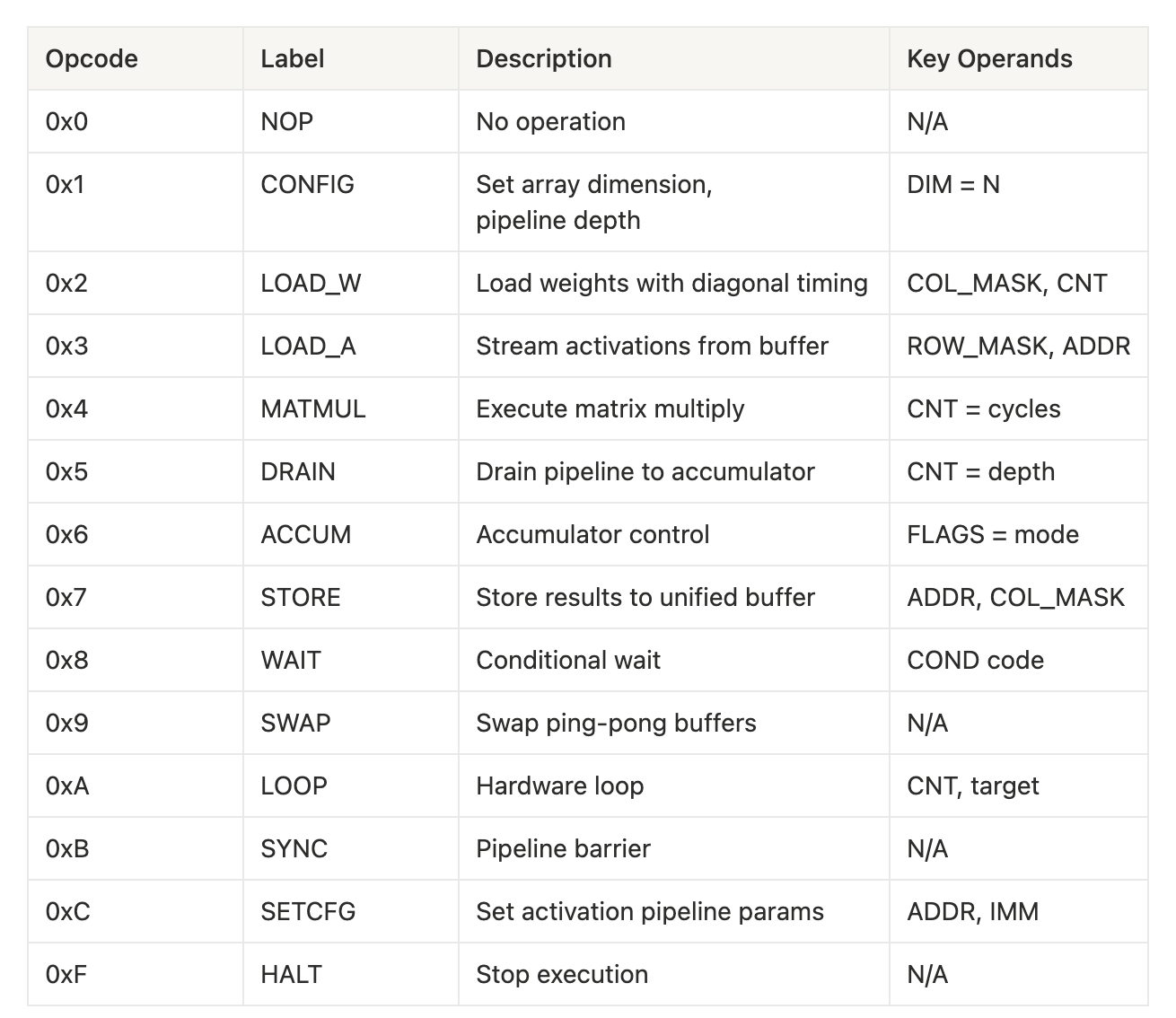
As an example, take a load weight instruction “LOAD_W” such that the column is masked with all eight columns and a count of nine. By concisely combining the intent using just one instruction, there is no need to further expand this into nine individual clock cycles and pass control signals in between these cycles. For, say a compiler targeting the tiny^2 TPU, the compiler can reason about operations at the matrix level without racking individual PE states or cycle-by-cycle timing. Instead, the compiled program can run correctly via timing expansion happening in hardware without the instruction stream.
Going Deeper: Automatically Microcode Generation
Once the instruction decoder receives a high-level operation from above, we expect to run a parametrized FSM that generates the appropriate clock cycle count and control signals for each clock cycle.
Dependent on the dimensions of an N x N systolic array, we sketch out:
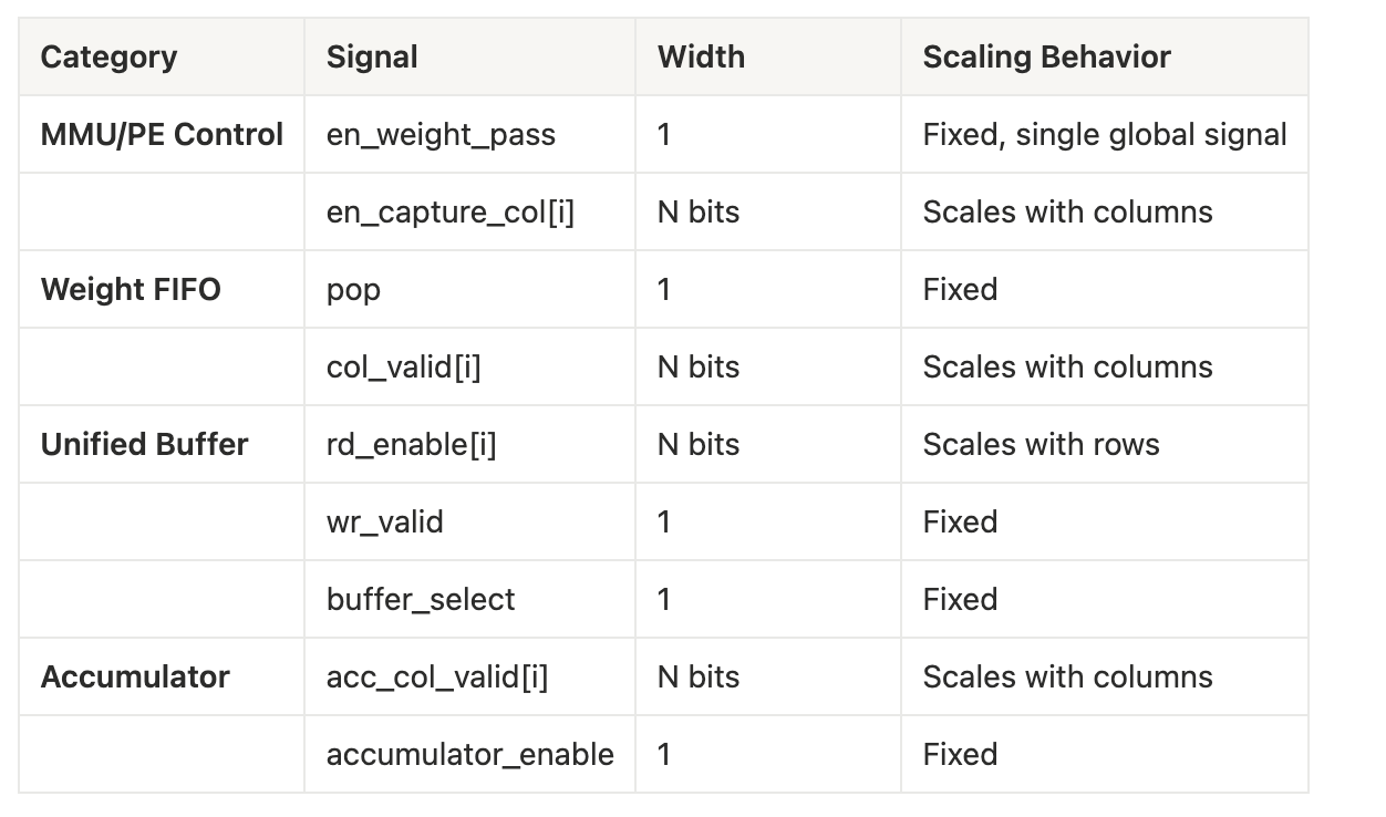
Taking weight loading operation from above continued as an example, this microcode generator pops from the Weight FIFO each cycle while asserting en_capture_col for each column index “i” when the cycle counter is exactly “i+1” (staggered effect). Thus, the exact value of en_capture_col for each column is en_weight_pass && (cycle count == i + 1) && col_mask[i].
Subsequent compute phase operations follow the generator reading from the Unified Buffer with row staggering, such that the UB’s row read enable for row index “i” is compute_phase && (cycle count ≥ i + 1) && (cycle count < (N+i)) && row_mask[i].
Streaming through the MMU, we envision the resultant accumulator valid signals follow the same pattern such that column index “i” of the MMU is valid when cycle count fully traverses the MMU systolic array. Thus, for every index of the MMU array each of these relationships between Weight FIFO and UB are repeatable boolean chunks of logic.
This concludes our rough draft of the tiny^2 TPU ISA.
Defining the ISA properly is extremely important as a good ISA is much cheaper than a good microarchitecture and the ISA directly dictates “design space of possible implementations” (Chisnall). We definitely have some drawing board work ahead, but our larger ideas are hopefully encapsulated here today. Onwards!
Works Referenced
Chisnall, David. How to Design an ISA (2024). https://queue.acm.org/detail.cfm?id=3639445
Jouppi et al. In-Datacenter Performance Analysis of a Tensor Processing Unit